We have a few old SMA SunnyBoy solar inverters I'd like to interface with - so after some research, it looks like these can be interfaced with different types of technologies (including RS232 and RS485). The way this is achieved is via "PiggyBack" modules that are installed in the inverter to provide one of these interface types.
Before we proceed further with poking at the hardware, please keep in mind that these inverters have both mains voltage and the string voltage of your PV panels present. This voltage can easily be hundreds of volts DC! The connection between inverter and panels does not have an RCD. The panels will happily push current through you as long as the sun shines.
It is absolutely crucial that you completely disconnect the inverter from both mains and PV panels before even thinking about opening it. Additionally, the inverter has very large capacitors that need to discharge. Follow the instructions provided in the service manual. Do not open the inverter if you don't know what you're doing - get a certified electrician to help.
Taking a closer look at an RS485 PiggyBack
While one can find pictures on the internet and infer some information from installation manuals, it doesn't compare to having one in your hands. I luckily found an RS485 PiggyBack for a reasonable price on ebay and it even included all accessories and manuals.
Here it is:
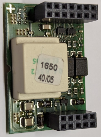
The construction is clearly built around a large isolation gap in the middle, where we only have optocouplers and a transformer going across. There's even a slit below the optocouplers and the copper layers are pulled back.
On the upper side (with the 2*7 pin header), we have two large ICs:
- a MAX253 transformer driver for isolated power supplies designed for isolated RS485 interfaces
- some variant of an AHCT14 inverter with Schmitt-Trigger inputs
There are also two SRV05 ESD protection diode arrays (the small 6 pin ICs) and some passives. This looks very much like the "hot", inverter side.
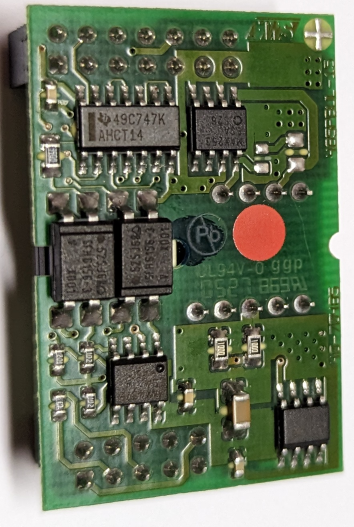
On the bottom side (with the 2*5 pin header), there are also 2 large ICs:
We also have a couple of diodes and larger capacitors - these are part of the secondary side of the transformer isolated power supply. They pretty much follow the example circuit from the datasheet of the MAX253.
In general, it looks like this board is designed to take the interface and power from the inverter, isolate it and provide RS485 on the bottom header.
Where does it all plug into?
The inverter has the matching headers to plug it in:
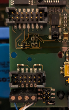
We can again see that the upper part is connected to the rest of the inverter, while there is a large isolation gap around the lower header.
The screw terminal is labelled "2 3 5 7" and is used to connect the RS485 interface. The jumpers next to it can be used to enable 680Ω pull ups / downs and a 120Ω termination resistor. The 680Ω resistors can be seen on top of the header. The 120Ω resistor is not present on the inverter side (but can be found on the PiggyBack)
We can get the screw terminal assignment from the installation manual. The positions are used differently if we compare the manuals from the RS232 and RS485 PiggyBacks. The connections between screw terminal and pin header are quite easy to determine with a multimeter:

| 2 | 3 | 5 | 7 | |
| RS485 | DATA+ | GND | DATA- | |
| RS232 | RX | TX | GND |
Some pins seem unconnected - but based on installation manuals, it looks like other devices also supporting PiggyBacks have wider screw terminals. Maybe these pins are connected in those devices.
Just visually speaking, it looks like screw terminal positions labelled 2 and 7, so the DATA signals for RS485 are best suited for differential signals, as they are of similar length and only 7 has a short (5mm-ish) stub to the side for the jumper.
It's also interesting how there's a mix of resistors on the inverter and on the PiggyBack - naively I would assume that you'd just want to have connections to the jumpers and then supply any required resistors on the PiggyBack. It could however be that either for space constraints or signal conditioning this arrangement worked better.
For the 680Ω pull up, pin 2 on the lower header has to be supplied with 5V from the LDO. To protect against improper installation, the pin is connected via two 100Ω resistors in parallel to limit the current as well as a diode to avoid reverse current flow.
Pinout of the Hot Side
Trying to figure out the pinout of the hot side, we immediately have obvious candidates for power and ground:
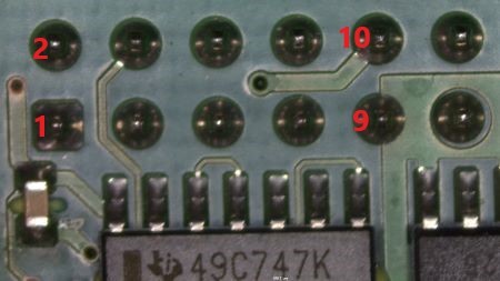
Pin 10 has a thicker trace than the others, and pin 9 is fully connected to something kinda ground-plane-looking. We can easily confirm with a continuity test to the power and ground pins on the MAX253 given in its datasheet.
Since I do not want to mess with my inverter under power, I don't know whether power is 3.3V or 5V. All ICs work with both voltages. Another trick to see which one works is to just power the board with 3.3V and seeing whether the secondary side gets enough voltage for the 5V LDO to work. Unfortunately the transformer is wound to give a slightly higher voltage on the secondary and both 3.3V and 5V create secondary voltages acceptable for the 5V LDO.
For the other pins its best to work our way backwards. From the MAX487E we know which pin is what. We essentially have 4 signals:
- RO: Receiver Output. This is the data received from RS485.
- RE: Receiver Output Enable. Can be used to put RO into high impedance mode.
- DE: Driver Output Enable. Has to be high to enable data transmission on RS485.
- DI: Driver Input. This is the data sent to RS485.
Note that RE, DE and DI all have to be driven by the inverter side, while RO is the only signal in the other direction. This matches up with the optocouplers: 3 of them point from inverter to isolated side, while only one goes in reverse.
Following the signals, they all cross the optocoupler, pass through the Schmitt-Trigger inverters at least once, go through a protection resistor, pass by the ESD diode array and end up on the pin header. The mapping on the header ends up being:
- RO: Pin 3
- DE: Pin 4
- DI: Pin 5
- RE: Pin 7
- GND: Pin 9
- VCC: Pin 10
In terms of the other pins, it looks like some can optionally be connected via unpopulated resistor footprints. Only pin 13 is connected via a 0Ω resistor to an inverted version of DI. No idea what that's used for, maybe some feedback to see if the PiggyBack is present / working?
Mechanical Aspects
Finally, a short note on the mechanical aspects: The hole in the inverter housing seems to be sized for a PG16 cable gland. Since that is a bit wide for the cables used in RS485, a reduction to PG11 and a PG11 cable gland are actually used.
Since the cable is likely going to touch the main DC input assembly, a silicone tube is provided to add further insulation between the data cable and the rest of the inverter. Depending on the insulating material and thickness of the data cable you use, this could actually be necessary to provide the required insulation - after all, it would be a bit silly to add this many protection mechanisms on the PiggyBack to then have a poorly insulated data cable rest directly on the high voltage carrying parts.