After my recent success with using AI to work on managed network switch firmware, I started experimenting more with how I could get Gemini CLI or Claude Code to do all the hard work for me to get OpenWRT ported to such devices.
I did eventually manage to get a mix of both these AI agents to get full support for the Horaco ZX-SW82TS-L2P including all LEDs, ports and PoE - but it involved hours of trying to coax the agents to make progress. While Claude Code tended to be better at managing knowledge and staying on track, it also burned through tokens and overage credits much faster than Gemini. During those experiments, I noticed that what you get out of Gemini depends a lot on the context and environment setup. So I wanted to try again on a different device.
The Horaco ZX-SWTG2C8F
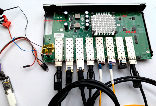
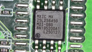
This is a managed 8 port SFP+ switch. Opening it up, we can again immediately spot the familiar SPI flash chip due to the larger and smaller package options.
We can also see 2 RTL8231 GPIO expanders and what looks like an unpopulated RJ45 footprint that could be meant for a console port as we saw on the other device. Next to it, we see an unpopulated IC footprint - if you have some experience with hardware you might already guess what this is for, but we can also take a picture and ask Gemini, which will hopefully tell you that this looks like a typical setup for a MAX232 IC with its charge pump capacitors next to it.
Based on the MAX232 datasheet, we can identify the pins that correspond to the TTL
side TX and RX pins. Soldering some fine wires to it and hooking it up to the oscilloscope
reveals 3.3V UART signals - yay! With a suitable UART->USB adapter, we can start poking
around and this time it even looks like rtk network on and tftpboot work out of the
box.
The Harness
Since the goal is ultimately to let Gemini perform the work on its own, just hooking up serial isn't enough - we also need a way to reboot the device without me manually unplugging the power each time. I had a spare IKEA Zigbee smart socket, so I used that to power the switch. In combination with Zigbee2MQTT this lets me power cycle the switch without touching it.
The Porting Environment
Let's collect what information we have:
- The firmware dump we got from the SPI flash
- The GPL release for a similar-ish ZyXEL device
- The GPL release for a similar-ish D-Link device
- U-Boot upstream sources
So let's start to organize a little directory structure for our workspace:
.
├── ghidra
│   └── ghidra_12.0.4_PUBLIC_20260303.zip
├── ghidra_projects
├── realtek_sdk
│   ├── dms-1250-oss-release
│   ├── README.md
│   ├── u-boot
│   └── zyxel-xgs-oss-release
├── SWTG2C8F
│   ├── NOTES.md
│   ├── openwrt
│   ├── PATCHES.md
│   ├── SWTG2C8F.bin
│   ├── TASKS.md
│   ├── TESTING.md
The idea here is that at the top-level, we have generic tools and reference material that is not specific to the switch only. You might have noticed I also just threw in the current release .zip file for Ghidra in case some binary analysis is necessary. In the switch-specific directory, we have a git clone of OpenWRT, the firmware dump, and some empty Markdown files we'll instruct Gemini to use for managing knowledge.
Now you likely could get going already with this - but typically the agents will struggle with managing context - particularly around the SDKs or the monolithic SPI flash dump. So first, we need to spend some time making this information digestible.
Mapping out the SDK
First, let's go into the realtek_sdk directory. We can leverage Gemini to populate a README.md file
that helps Gemini itself to better understand the SDKs and the key information. I used this prompt to
get started:
This directory contains 2 directories (dms-1250-oss-release, zyxel-xgs-oss-release) containing GPL
releases of switch firmware, containing the Realtek SDK. A 3rd directory "u-boot" contains the upstream
u-boot repository checked out at the v2011.12-rc3 tag which should most closely match the U-Boot version
used in the Realtek SDK. Your task is to create a README.md file that describes and compares the contents
of each oss release. It might be beneficial to index the code with GNU global to make cross referencing
more efficient. The resulting README.md should allow a skilled firmware engineer to quickly browse code
to understand how hardware initialization, device support, etc. works
and finding the relevant code efficiently. This should greatly simplify implementing device support for openwrt.
This already generated a great overview, but was lacking a bit of detail in pretty much all of the sections. So I followed up with:
We'll now expand some sections. Remember to keep referencing concrete source code files or even code
excerpts to make the information is to understand and cross-reference. First, let's dig deeper on the
Bootloader. Figure out what custom commands, image headers or other notable things on top of u-boot's
upstream behavior have been customized. Extend README.md to fully document these customizations.
Which worked out great, and you can just keep doing this, asking it to expand section after section - for example, my next prompt was:
Great findings! Dive even deeper: Expand the README.md further on how flshow works, where it gets the partition layout
from, etc. Then also spend some time to understand how the LED configuration in the hardware profile works and how
GPIO expanders or shift registers or similar play their part. Remember to keep referencing code.
and
Awesome. Now let's move on to the linux kernel customizations. Analyze any behavior of interest for porting efforts
and document them, referencing code. Pay special attention to: How flash access works, MTD driver, partitons etc.
The rtcore.ko / rtk.ko or other custom kernel modules and any other customizations.
Gotta give some positive reinforcement every once in a while ;) The references to these kernel modules could be considered cheating a bit, since I saw these in my earlier work with the other switch where they were visible on the console log.
Now that we have this detailed README.md, we can just refer to it in the future, which will cause Gemini to just load this into context, giving a bit of a map to the SDK and it finds relevant information much faster.
Picking apart the Firmware
Now moving on to the firmware dump, the biggest challenge is to properly split it into the different MTD partitions and extracting the kernel and root filesystem. Often binwalk is used for this, but with this switch in particular, I got imperfect results. Since we know a lot about the structure from the Realtek SDK, we should be able to perfectly split up the pieces and extract everything properly instead of going by pattern matching and heuristics.
My goal here was to have Gemini create a set of scripts I can use to
do the extraction. The first was extract_kernel.py, where I asked for a script scanning for the U-Boot Linux image
header, accounting for the custom magic value the Realtek SDK sets (thus breaking binwalk). This took quite a bit
of handholding, but it let me focus on the tricky parts while Gemini took care of the boring code. The result
was a script that reliably extracts the linux image and rootfs for all firmware dumps of similar devices I have.
The next script, kernel_partitions.py is a bit more adventurous and I did not bother trying to understand
how Gemini actually pulled it off - but I was essentially asking for some automated analysis of the linux image
to find the baked in MTD partition table, by looking for known partition names like LOADER or BDINFO. This
was very unreliable at first, but having it constantly verify the results against all firmware dumps I had
eventually led to something that worked on all of them.
I have also experimented with getting this from U-Boot, but Gemini struggled a lot with the different addressing modes U-Boot goes through, where the same location in flash can be accessed by about 3 different address ranges depending on what stage during boot we are in.
With these two scripts and a hwprofile extraction script I had Gemini write for the previous device work, we have more stuff in our device directory:
├── SWTG2C8F
│   ├── BDINFO.bin
│   ├── hwprofile.c
│   ├── JFFS2_CFG.bin
│   ├── JFFS2_LOG.bin
│   ├── LOADER.bin
│   ├── NOTES.md
│   ├── OEMINFO.bin
│   ├── openwrt
│   ├── PATCHES.md
│   ├── rootfs
│   ├── RUNTIME.bin
│   ├── SWTG2C8F.bin
│   ├── SYSINFO.bin
│   ├── TASKS.md
│   ├── TESTING.md
│   └── vmlinux
Interaction with the Serial Port
Gemini is not fast enough to directly mess with the serial port - especially since we have just about a second or two to interrupt booting and getting to the U-Boot prompt. So we need some sort of manager process that takes care of the resetting and entering U-Boot while providing a simple CLI for Gemini to use.
I first tried a somewhat simple prompt just describing the problem - and it came up with something that worked. It was however plagued by timing issues and often Gemini would fall into a loop of trying to boot a custom built OpenWRT image, it not working for some timing issue and then Gemini trying again with artificially large sleep calls injected. This was good enough to actually perform all of the porting work but it was very slow and annoying.
What worked much better was writing out a design in Markdown and then just telling Gemini to implement that and verifying against a real device. You can see the design here and the resulting one-shotted script here.
I created a TESTING.md file which just contains a brief comment about how to use the script
and the necessary values for MQTT server, topic and serial port to use, as well as where
to put the built image to serve it over TFTP and how to boot it in U-Boot.
The Porting Process
So with that, we have:
- A lot of supporting material with the SDK sources
- The firmware split apart into nice chunks
- An OpenWRT checkout to work on
- A way to test on real hardware
So let's get started. This is the prompt I used:
We're working on reverse engineering a managed switch firmware in the SWTG2C8F directory.
It uses the Realtek SDK, for which we have sources from similar devices in the realtek_sdk
directory - see the realtek_sdk/README.md file to understand how it is generally structured.
In SWTG2C8F, I have already extracted the different MTD partitions into separate .bin files,
the kernel into a vmlinux file and the root filesystem into the rootfs directory. We also
have a heuristically extracted hardware profile in hwprofile.c. Now we're still missing some
clarity especially around the two RTL8231 chips on the board - they are presumably used for
LEDs and/or I2C or control signals for the 8 SFP+ cages on the switch. Your task is to examine
the firmware and devise a strategy on how we can determine the missing information needed to
come up with a functioning device tree and eventually OpenWRT port. Keep notes from your analysis
in SWTG2C8F/NOTES.md. Constantly revise and extend NOTES.md after every insight and discovery.
Also keep a TASKS.md file with tasks that you want to defer to later or to capture open questions.
If you think extra tooling is needed, propose what we'd need and how to set it up.
And off it went. It independently found the board_conf.ko kernel module where it found a lot
of information about this specific switch. After a while, it was satisfied with the information
extract regarding the SFP ports, proposed next steps and stopped. I just told it to continue with
those next steps.
After a while, it seemed like it collected all the necessary information. I then prompted it to start the porting work:
Alright, I have now cloned the openwrt git repository into SWTG2C8F/openwrt.
Add support for our device in the proper place for realtek targets. There's been a lot of recent
work on realtek devices, so examine the recent git log to understand the changes. When creating
the device tree, ensure you use a modern style, using the existing port macros etc where appropriate.
The flash layout should be compatible with the vendor firmware, i.e. leave LOADER, BDINFO etc alone
and only use the RUNTIME partition for openwrt. Finally, build the initramfs style image so I can
attempt to tftboot it. If compilation fails, fix any issues encountered. Remember to keep taking notes if you
learn anything new.
I didn't quite tell it about the hardware access at this point since I wanted to test it myself first. There were some glaring issues at first around the memory layout (it just assumed a larger amount of memory) which I went back and forth on manually for a while. But eventually I told it about the TESTING.md file and it started happily iterating on its own and I didn't pay that much attention anymore. Occasionally, you could just hear the relay in the smart socket click, when it did another reset and boot cycle.
A big challenge was again dealing with the RTL8231 GPIO expanders, which already turned out to be a huge pain
the last time around. These devices can run in multiple modes and the RTL930x has some integrated support for
driving LEDs / polling them independently. I think Gemini eventually resorted to running rtk network on and
then dumping memory registers via the U-Boot prompt to reverse engineer the configuration.
While Gemini can get a lot done independently with a setup like this, it still occasionally requires some steering. It seems to sometimes fall into a somewhat cyclic trial and error mode. You can break out of this by giving instructions on where to look for information next. For example, specifically telling it to use Ghidra in headless mode to analyze a binary.
Something that also works really well is to ask for verification of the work with specific measurable
goals. For example, for a while, it struggled to get the I2C busses set up correctly. Saying that all
SFP+ cages have modules inserted and to build an image with the full ethtool to read out the SFP
modules worked wonders - it first got port 1 working but struggled with the rest, then eventually got
all of them working.
Conclusion
Using AI agents to work on device support has made it more accessible for me, as I no longer have long, uninterrupted chunks of time I can just stay focused on reverse engineering these days. With AI, I just have to manage the overall process and goals, while AI does most of the heavy lifting.
In this case, it easy somewhat easy mode since there are released SDK sources under GPL for very
similar looking devices, but I'd hope that the more general reference material, SKILLS.md and tooling is built,
the better this process also works without these.